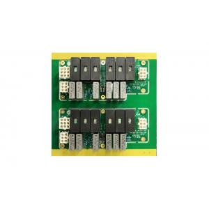
Ceramic Min Space Computer PCBA Prototype Fast BOM File Made
Shenzhen Yideyi Technology Co., Ltd specialize in prototyping & OEM and small-volume production, making your requirment complete on the one-stop destination of boards fabrication and assembly.
EMS include consumers electronic ,medicla, industrial,power control, automotive. Temperature & Humidity ,Internet & Communication Smart Home Security etc device .
Our Advantages:
1. Quick lead time of prototype & Punctual delivery.
2. Think highly of quality -- High pass rate
Pass rate of prototype: 100%
Pass rate of mass production: over 99.95%
3. Provide free consultation service of PCB and PCBA design.
4. No MOQ: we accept small order as well as bulk order.
5. Certification: Rosh, Reach, ISO 9001, 14001, UL, etc.
6. Provide OEM and ODM service.
PCBA Capability
| | Normal FR4,Normal Tg FR4(Halogen free),High Tg FR4(Halogen free),HDI PCB material |
| | Rigid pcb(Backplane,HDI,High multi-layer blind&buried PCB,Embedded Capacitance) |
| | Blind&buried via type,HDI PCB |
| | Lead free,Leaded,aspect ratio,Max finished size,MIN finished size, PCB thickness, MAX high to gold finger |
Plating/coating thickness | Tin thickness,OSP, ENIG, Immersion Silver,Immersion Tin,Hard gold, Soft gold |
| | MAX thickness of mechanical hole 4mil/6mil/8mil,Min/Max laser drilling size,Finshed mechanical hole size |
| | Min Pad size for laser drillings,Min Pad size for mechanical drillings,Min BGA pad size,Pad size tolerance(BGA) |
| | MAX drilling tool size for via filled with Soldermask (single side) |
| | Min gap between mechanical hole wall and conductor (Local mixed pressure area) |
| | Layer counts,PCB size (Finished),MAX PCB size(Ceramic-substrate PCB),PCB thickness(Finished) |
| | Min space of the V-CUT does not reveal the copper ( Central Line of v-cut to internal/external circuits,H means board thickness) |
Exquisite Technics
Having been specilezed for 13 years we understand the 3 high goals that are most concernd about your important stage from R&D to project manufacturing.
Engineer, procurement and quality department import product files on the production site. Priduct quality is determined by the import of product data in the early stage.

We provide superior service for automotive electronics, medical electronics, telecommunications, industrial control, smart home and other industries around the world
FAQ:
Q1. How to you make the impedance calculation?
The impedance control system is done using some test coupons, the SI6000 soft and the CITS 500s equipment from POLAR INSTRUMENTS.
The equipment measures the impedance on a representative track configuration coupon of which the client has given us a determinate value and tolerance.
Q2. What kind of PCB file format can you accept for production?
Gerber, PROTEL 99SE, PROTEL DXP, CAM350, ODB+(.TGZ)
Q3. How do we ensure quality?
Our high quality standard is achieved with the following.
1. The process is strictly controlled under ISO 9001:2008 standards.
2. Extensive use of software in managing the production process
3. State-of-art testing equipments and tools. E.g. Flying Probe, X-ray Inspection, AOI (Automated Optical Inspector) and ICT (in-circuit testing).
4. Dedicated quality assurance team with failure case analysis process
5. Continuous staff training and education
Q4. How can we guarantee you receive an good quality product?
For PCB, we will use Flying Probe Test, E-test etc. for it.
For PCBA, we need you to offer us a method or test fixture for the function test.Before that, our inspectors will use microscope and X-ray to check the IC footwelding or bad solder etc.
Q5. What’s the key equipments for HDI manufacturing?
Key equipment list is as following: Laser drilling machine, Pressing machine, VCP line, Automatic Exposing machine, LDI and etc.
Q6. What’s the typical process flow for multi-layer PCB?
Material cutting → Inner dry film → inner etching → Inner AOI → Multi-bond→ Layer stack up Pressing → Drilling → PTH → Panel Plating → Outer Dry Film → Pattern Plating → Outer etching → Outer AOI → Solder Mask → Component Mark → Surface finish → Routing → E/T → Visual Inspection.